TMCnet News
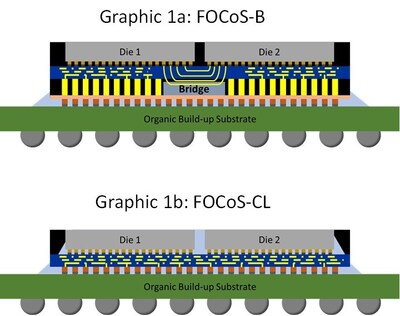
Sarcina Unveils Bump Pitch Transformer CapabilitiesNew Multi-die Technology Radically Alters 2.5D Packaging Landscape PALO ALTO, Calif., June 18, 2024 /PRNewswire/ -- Sarcina Technology, the Application Specific Advanced Packaging (ASAP) Design Service and Production leader, today unveiled its Bump Pitch Transformer design capabilities that slash 2.5D packaging NRE and production costs while significantly reducing design cycle time. The new technology will open new artificial intelligence computing opportunities. Sarcina's Bump Pitch Transformer, which is a silicon bridge technology, replaces expensive silicon TSV interposers with more cost-effective re-distribution layers (RDL). This architecture is ideal for homogenous and heterogenous chiplet integration targeting high-performance computing (HPC) devices for AI, data center, microprocessor, and networking applications. "We believe that the Bump Pitch Transformer architecture will accelerate the growth rate of 2.5D semiconductor packages that are key to meeting the explosive demand for AI-driven computing capabilities," said Dr. Larry Zu, Founder and CEO, Sarcina Technology. Current advanced 2.5D packaging necessitates the use of a substrate to transpose the microbump pitch fom 40-50 mm to 130 mm. These substrates are very expensive, in short supply, and are complex to design resulting in lead-time and cost challenges for many AI system companies. The Bump Pitch Transformer is effectively a Wafer Fan-out RDL technology which due to its maturity has inherently a lower cost and shorter lead time thus enabling system designers to optimize AI for new lower cost applications. Sarcina is currently engaging customers with two Bump Pitch Transformer derivatives across a range of applications. One derivative creates a silicon bridge in high density applications to connect the I/Os of adjacent dice. Tall copper pillars with a pitch of about 130 mm will be grown underneath the RDLs. Because the majority of the I/O interconnections are between adjacent dice and have been connected by the silicon bridge, a fewer number of I/Os need to be routed to the next level of interconnect with 130 mm bump pitch with tall copper-pillar bumping onto a standard substrate for flip-chip assembly. The RDLs will merge power and ground micro-bumps with 40-50 mm bump pitch, reducing the number of power and ground bumps with tall copper pillars suitable for 130 mm bump pitch density. These bumps may also be assembled onto a standard organic or laminate substrate for flip-chip assembly. "Today's substrate fabrication and package assembly technologies can't handle such a small micro-bump pitch without a bump pitch transformer. They can only handle approximately a 130 mm copper-pillar bump pitch. Secondly, adjacent die-to-die interconnections require a higher routing density to handle a 40 mm micro-bump pitch with several thousand I/Os," explained Dr. Zu . Sarcina also provides a "chip last" service, that handles die-to-die interconnects with less interconnection routing density. The company is prepared to accommodate a broad range of interconnect densities across both assembly technologies. About Sarcina Technology Founded in 2011, Sarcina Technology is the Application Specific Advanced Packaging Service that provides a boutique collaborative experience for small-to-mid-sized IC companies. It boasts a proven 100% right-the-first time advanced packaging track record of wafer-to-production services that reduce overheads and speeds time-to-volume. For more information, visit sarcinatech.com.
SOURCE Sarcina Technology LLC 
|


